


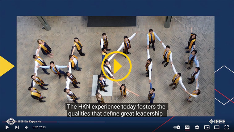
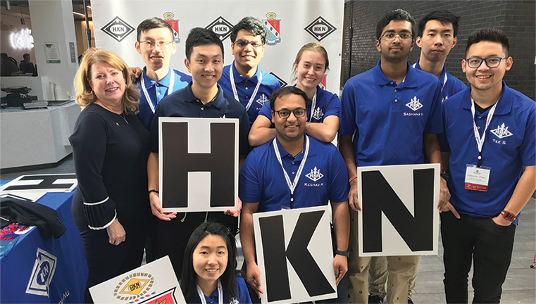
IEEE-Eta Kappa Nu (IEEE-HKN), the honor society of IEEE, promotes excellence in the profession and in education with ideals of Scholarship, Character and Attitude.
Founded on 28 October 1904, HKN promotes professional accomplishment, service to others, and leadership development for students and professionals in electrical engineering, computer engineering, and other IEEE fields of interest. With its merger in 2010 with IEEE, the honor society now has over 200,000+ members in more than 250 Chapters around the globe.
Chapters
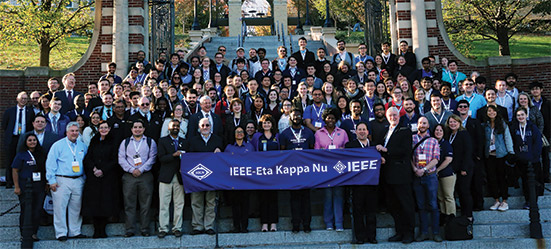
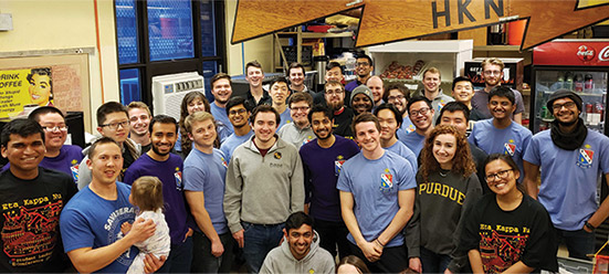
The 250+ IEEE-HKN chapters worldwide are your local link to the valuable resources offered by IEEE-HKN. Get involved to build your leadership, technical, collaboration, and communication skills.
Alumni
Once HKN, always HKN. Be a part of our 30,000+ active alumni members. Stay connected, recruit from HKN’s pool of stellar applicants, be a life-long learner and mentor. In other words, live out the HKN values.
Professional Members
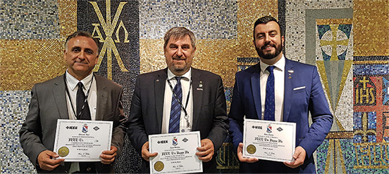
IEEE-HKN can be your technical and professional home. Professional members are individuals who have set themselves apart through their outstanding work and contributions to the IEEE fields of interest. Find out how to become part of this vibrant global community.
Eminent Members
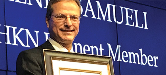
The society’s highest membership classification, HKN Eminent Member, is conferred upon those select few whose attainments and contributions to society through leadership in the IEEE technical fields of interest have resulted in significant benefits to humankind.
269
Chapters
100000
Service Hours
3000
Annual Inductees


Invest in
Our Community
Our Community
Your donation helps us provide critical chapter support to ensure that every student has the best possible experience. It provides the opportunity for every chapter to attend our life-changing Student Leadership Conference, increases service and career opportunities for our expansive alumni network, and so much more.
Strengthen
Our Chapters
Our Chapters
Our Chapter Support Initiative fuels the innovation and ingenuity of our student members through two key programs: the IEEE-HKN Chapter Support Grant Program and the IEEE-HKN Chapter Success Program.
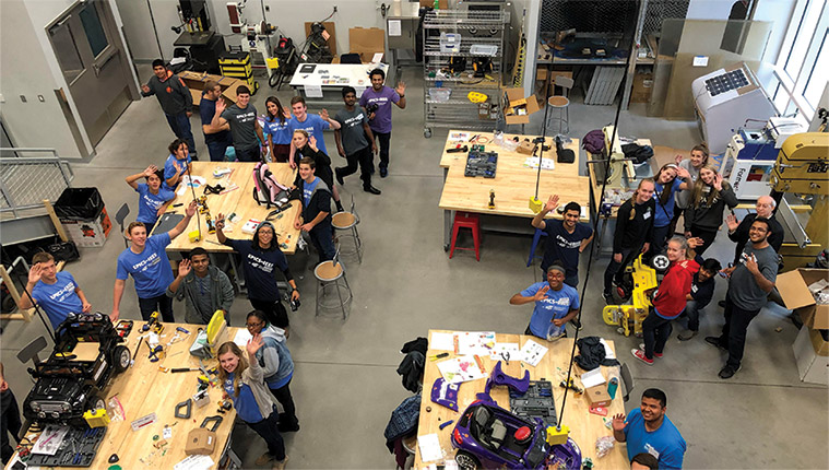
Empower
Our Students
Our Students
IEEE-HKN develops promising young professionals into the engineering and technical leaders our world needs. The annual IEEE-HKN Student Leadership Conference, through dynamic programming, sparks a lifelong spirit of service in attendees, grows their technical aptitudes and leadership skills, prepares them for the next stages of their careers, and fosters connections that last a lifetime.Your donation will open this opportunity to more students.
Power
Alumni Connections
Alumni Connections
Be the force behind HKN’s vision for an interconnected alumni network that any member, anywhere can activate at any stage in their careers. Build local and global networks, and invest in the people and ideas that will change our world.
News & Updates
Eclipse Day was extra exciting for Eta Kappa Nu! A new University Chapter joined the community just before the celestial event made its way to the eastern US. Welcome to the HKN family, Lambda Chi Chapter of Hampton University! …
HKN had a busy weekend at IEEE SoutheastCon last month! At our first Professional Induction of the year, we welcomed three new Professional Members to the Eta Chapter. Congratulations to Brian Page, Dr. Masood Ejaz, and Professor Arup Kumar Ghosh…
As you know, HKN is on a roll this year, especially in Region 9 (Latin America)! Our second Chapter in Puerto Rico was installed on Friday, 22 March 2024 at Polytechnic University of Puerto Rico in San Juan! Welcome to…
Episode 9 of IEEE-HKN Career Conversations is here with engineer, academic, and consultant, Jacquelyn Nagel, Ph.D.! You won’t want to miss this episode focused on finding inspiration, bio-inspired design, and cultivating curiosity and creativity! Check it out >>
THE BRIDGE
IEEE-Eta Kappa Nu (IEEE-HKN)’s signature publication, THE BRIDGE, is an interactive digital magazine published three times a year.

